Near-field nanofabrication and photophysical probing of organic semiconductor nanostructures
This project is funded by the Interdisciplinary Research Collaboration between the Universities of Cambridge, Bristol and UCL, and aims to combine the manufacturing and the investigative capabilities of scanning near-field optical microscopy (SNOM) with time-resolved optical spectroscopy to develop fabrication technology, advanced applications and fundamental understanding of organic semiconductors nanostructures. Other collaborators involved with this project are Dr Carlos Silva and Professor Richard Friend at the Cavendish Laboratory (Cambridge) and Dr Mark Blamire in the Department of Materials Science at Cambridge.
Organic semiconductors have come under intensive investigation in the last 10 years because of their novel physics and the unusual possibility of cheap fabrication of large area optoelectronic devices, such as light-emitting diodes (LEDs), photovoltaic diodes (PVDs) and transistors, via technologically robust solution-process methodologies (spin-coating, ink-jet printing etc.).
Nanostructures of such semiconductors are interesting for several reasons. For example, patterning so as to achieve a modulation of the refractive index in the 100 nm lengthscale can be used to modify the photon density of states (DOS), thus allowing the fabrication of so-called "photonic structures" [1]. The latter can be used to improve the luminescence internal quantum efficiency (because of the alteration of the photon DOS and thus of the radiative rate) and/or to improve the out-coupling factor (by reduction of waveguiding), as well as for low-loss routing of optical beams through bends and curved paths in optical chips. Conventional lithographies are not ideal for conjugated polymers, which are prone to degradation in some of the processing steps. A possibility for circumventing this problem is the direct writing of structures in photosensitive conjugated polymers, which is described below in more detail. However, far-field illumination is not ideal, as the resolution is limited by the Abbe diffraction limit, and because the absorption features of the material may not be ideally matched to the wavelength needed for the resolution. This is a strong point in favour of illumination through a SNOM tip. In such case, in fact, the illumination photon energy can be tuned to match the absorption properties of the materials, with the resolution set independently by the probe aperture size.
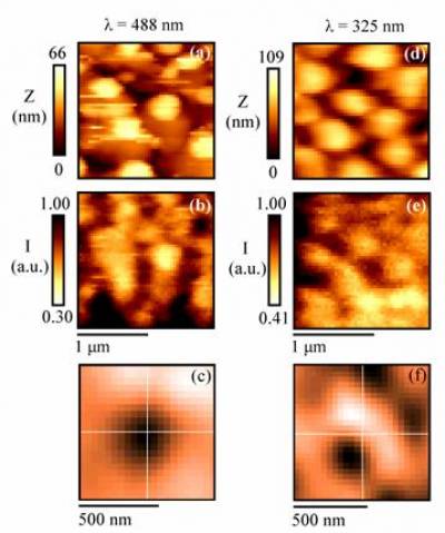
The small entropy of mixing of polymers leads, naturally, to self-organisation and phase-separation of heterogeneous polymer blends processed from the same solution, with domains size from few nm upwards. When suitable semiconductors are selected, these are nanostructures with significant electronic functionality. For example, in photovoltaic diodes, important parameters are the energy level offsets between the highest occupied molecular orbitals (HOMO) and the lowest unoccupied molecular orbitals (LUMO) of the different polymers. When such offsets are large enough exciton dissociation at the polymer interface is energetically favourable. Optimum balance between phase-separation on a fine scale (~10 nm) to achieve a large charge transfer yield, and phase segregation on a longer length scale to allow efficient charge percolation to the appropriate electrode, and avoid efficient geminate recombination, must also be achieved to ensure efficient photovoltaic conversion [2-3]. Similar nanostructures can also be important for LEDs. For example, the use of blends allows separate optimisation of electron/hole transport and luminescence efficiency, often impossible in a single material. The phase separation and subsequent increase of interfacial area can also favour the recombination of oppositely charged carriers to form excitons, if the sum of the energy levels offsets is smaller than the exciton binding energy. Since many of these phase-separated features are smaller than the resolution achievable with far-field microscopy, a SNOM system, with capabilities for both manufacturing and characterisation on a sub-wavelength scale, is a powerful instrument to assist further development of the nanotechnology of organic semiconductors. An obvious advantage over AFM is chemical contrast, which allows the straightforward discrimination between different materials (e.g. in a multi-phase) by their spectral properties [4]. This is illustrated in figure 1 below, that shows topography and fluorescence images of a phase-separated thin film of a blend of 2 different polyfluorenes (namely poly(9,9'-dioctylfluorene), PFO, and (poly(9,9'-dioctylfluorene-alt-benzothiadiazole), F8BT) excited at 488 nm and 325 nm.
Figure 1: (a,d) Shear force topography and, (b,e) SNOM fluorescence of a PFO/F8BT blend thin film, measured using 488 nm excitation (a,b) and 325 nm excitation (d,e). Note that fluorescence is from F8BT, either following direct excitation, or after energy-transfer from PFO, whose fluorescence could not be detected. Contrast has been inverted in (b,e) to facilitate correlation of fluorescence and topography. Regions of intense fluorescence appear black. (c) Correlation plot for images (a) and (b). (f) Correlation plot for images (d),(e).
Topographic images reveal a rich surface structure, with one phase forming circular regions 200-300 nm in diameter, protruding from the surface of the film, in agreement with previous AFM studies. Such protruding regions correlate with the areas of weaker fluorescence, indicating that they contain a smaller proportion of F8BT than the other phase. Since both excitations are absorbed predominantly in F8BT, it is not surprising that the results are qualitatively similar. Observation of some F8BT emission (30 to 40% of maximum), in the "low fluorescence" regions, implies the presence of F8BT also in PFO-rich regions.
White and black areas in the correlation plots (c,f) correspond to displacements of the optical with respect to the topographic image, resulting in a correlation (white) or anti-correlation (black) of protrusions with areas of intense fluorescence. In (c) the distinctive black circular region, centred at a displacement of ~40 nm, confirms that the protrusions of the film are less fluorescent. The white region, indicative of correlation for displacements of ~400 nm, is taken to represent the underlying regularity in the polymer film. The same pattern is repeated for 325 nm excitation (f), although here the displacement between protruding regions and areas of less intense fluorescence is greater, ~ 200 nm. This is consistent with the form of the SNOM probe used for these experiments. The observation of such a displacement provides a strong argument for rejection of topographic artifacts.
Fabrication and rapid prototyping of 2D photonic structures
In this context, we would like to use the SNOM as the manufacturing tool for a range of nanostructures to be "directly written" in photochemically active conjugated polymers or conjugated polymer precursors such as that of poly(p-phenylene vinylene (PPV). UV exposure of the solution-processable PPV precursor results in partial cross-linking which inhibits the solubility, thereby allowing direct lithography. A subsequent thermal annealing allows conversion of the patterned and partially cross-linked precursor to the conjugated polymer. The remarkable possibility of rapid prototyping of very different structures results from the direct writing capabilities. In particular, it is easy to fabricate in this way "periodic structures with intentional defects" (or "doped photonic crystals") which are interesting for control of the optical properties, and that would not be possible, for example, with holographic lithographies.
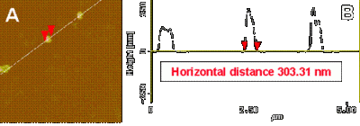
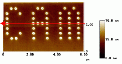
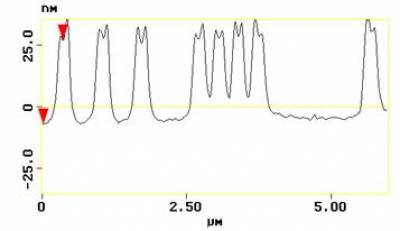
We will explore the fabrication of a variety of structures with different lattices, and in particular quasicrystal lattices [5], which allow fabrication of photonic band-gaps (PBG) still in the presence of moderate refractive index contrast, such as those expected for polymers. Fabrication is to be carried out in the Physics Department at UCL, by means of a home-built SNOM, whereas testing of the PL and of the lasing properties will be carried out in Cambridge (Physics), using a high-power femtosecond laser source broadly tuneable via optical parametric generation and amplification. The project also builds on the possibility of manufacturing high-quality SNOM-probes (see figure on the side, showing the probe aperture) by focused-ion-beam (FIB) processing to be carried out in the group of M Blamire (Cambridge - Materials Science). Proof-of-principle nanostructures fabricated with this system are reported in figure 2 and 3.
Figure 2: AFM topographic image (A) and cross section (B) of PPV pillars fabricated by means of SNOM lithography. Note the aspect ratio of nearly 1.
Figure 3: AFM image of an arbitrary pattern of PPV pillars prepared by SNOM lithography (top). The cross-section (bottom) is from right to left, as indicated by the red arrow on the left panel. Pillars with full width at half maximum (FWHM) down to 160 nm have also been produced (not shown).
Interface photophysics in semiconductor polymer blends and binary nanostructures investigated via near-field fluorescence and photoconductivity (PC) scanning microscopy
In addition to manufacturing, we would like to carry out preliminary work to gauge the potential in combining SNOM and other time-resolved spectroscopic techniques aimed at the characterisation of the photophysics of self-organised polymer nanostructures, with a special attention to the photogeneration processes occurring at heterogeneous interfaces.
We will investigate blends of poly(9,9'-dioctylfluorene), PFO, and derivatives including triarylamines (poly(9,9' -dioctylfluorene-alt-bis-N,N' -(4-butylphenyl) -bis-N,N' -phenyl -1,4 -phenylenediamine), PFB, and similar as well as benzothiadiazoles (poly(9,9'-dioctylfluorene-alt-benzothiadiazole), F8BT), which are promising for PVD and LED applications . The photophysics at organic-organic interfaces is of central importance in these systems, and we will focus on the role of interface-specific excited states in the electronic properties. In particular, it will be powerful to correlate kinetic information gathered using near-field TCSPC with steady-state PL and PC measurements made with SNOM using picosecond diode lasers, which have become available recently.
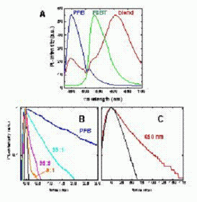
We will also apply far-field polarisation anisotropy TCSPC and TA measurements in blend grating structures achieved by solution embossing techniques, demonstrated recently (RHF), whereby structures with alternating alignment of different phases were achieved with nanoscale resolution. Preliminary far-field, time-resolved PL measurements on PFB/F8BT blends by CS and co-workers have established the strong contribution of exciplex species to the picosecond kinetics (Figure 4). This observation poses intriguing questions about the mechanism for charge photogeneration in polymer PVDs. Exciplex-like states may display a high degree of charge transfer character, such that they may be a major pathway for exciton dissociation. The role of interfacial states in the charge separation processes in a PVD will be explored by measuring local excited-state decay kinetics and correlating this key information with topography and steady-state PC.
Figure 4: (A) PL spectra of spin-coated films of PFB, F8BT, and of a PFB:F8BT blend (9:1, by weight). (B) Decay curves of the PFB emission (440 nm) in films of pure PFB and PFB:F8BT blends of various compositions. (C) PL-decay of the exciplex emission in the 9:1 blend.
References:
- J. D. Johannopoulos, R. D. Meade, and J. N. Winn, Photonic Crystals: molding the flow of light (Princeton University Press, Singapore, 1995)
- D.M. Russell, et al. Appl. Phys. Lett. 80, 2204 (2002)
- J. J. M. Halls, A. C. Arias, J. D. Mackenzie, W. S. Wu, M. Inbasekaran, E. P. Woo, and R. H. Friend, Adv. Mater. 12, 498-502 (2000)
- R. Stevenson, R. Riehn, R. G. Milner, D. Richards, E. Moons, D. J. Kang, M. Blamire, J. Morgado, and F. Cacialli, Appl. Phys. Lett. 79, 1921-1922 (2001).
- M. E. Zoorob, M. D. B. Charlton, G. J. Parker, J. J. Baumberg, and M. C. Netti, Nature 404, 740-743 (2000).
 Close
Close


