Scanning Near-field Optical Microscopy is a scanning probe technique which allows effective control and detection of electromagnetic fields (from IR to UV) below the diffraction barrier (i.e. below λ/2 in air), that is in the so-called "Near-Field". In solid state physics and more specifically in the area of organic semiconductors, this provides the unique opportunity for investigating, optically, mesoscopic phenomena which occur in homogeneous and heterogeneous structures (such as polymer blends). The SNOM is also a marvellous tool for studying and controlling the effect of topological and energetic disorder.
The project will focus on the investigation of organic semiconductors nanostructures for optoelectronic devices (mainly Light-Emitting Diodes and Photo-Voltaic cells) with the potential for improved control of both spectral/spatial distribution of luminescence and transport properties. The structures will be fabricated by exploiting self-organising processes (such as phase separation in polymer blends) and via other non-conventional lithographic techniques (e.g. soft-lithographies, see also the project: "Lateral patterning of Organic Nanostructures").
We have recently developed a method for using the high spatial resolution of the optical field of a SNOM probe to fabricate nanostructures of photosensitive conjugated polymers or of their precursor.Preliminary experiments focused on the electroluminescent polymer poly(p-phenylene vinylene), PPV. The technique is based on the spatially selective inhibition of the polymer-precursor solubility by exposure to the ultraviolet optical field present at the apex of near-field probes with aperture diameters between 40 and 80 nm (±5 nm). After development in methanol and thermal conversion under vacuum we obtained features with a minimum dimension of 160 nm.

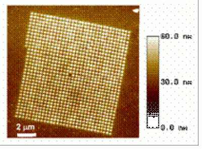
AFM image of a photonic crystal structure with intentional central defect, drawn in poly(p-phenylene vinylene) using UV light
Using a SNOM of our own design and construction we have carried out direct writing of two-dimensional photonic crystals with intentional defects and a periodicity relevant to applications in the visible range, such as the one shown in the figure above (period~330 nm, pillars FWHM~200 nm). With respect to other demonstrations of near-field lithography our uniqueness is in the ability to achieve features with substantially greater heights, aspect ratios, better "cleanliness" and definition, as well as in the fact that our final product is a fully conjugated, functional polymer. This work has also been highlighted in Materials Today, and Laser Focus World. We are now interested in taking this project forward via implementation of different schemes of high-resolution optical excitation and patterning, and in particular via use of an apertureless probe. Further details of the technique and its capability can be found in the following publications.
- R. Riehn, A. Charas, J. Morgado and F. Cacialli. Near-field optical lithography of a conjugated polymerAppl. Phys. Lett. 82, 526-528 (2003).
- F. Cacialli, R. Riehn, A. Downes, G. Latini, A. Charas, and J. Morgado. Fabrication of Conjugated Polymers Nanostructures via Direct Near-field Optical LithographyUltramicroscopy 100, 449-455 (2004).
- Riehn, R. Stevenson, J. J. M. Halls, D. R. Richards, D.-J. Kang, M. Blamire, A. Downes and F. Cacialli. Near-field photoconductivity of a polyfluorene based conjugated polymer blendAdvanced Functional Materials 16, 469-476 (2006).
 Close
Close

