The Science behind the research
Transparent Conducting Electrodes (TCEs) are widely used in optoelectronic devices like solar cells, light emitting diodes, liquid crystal display, and tough screens. With the ever increasing demand for these products there is significant research being conducted to enhance their performance through manufacturing process optimisation.
Currently both high temperature and low temperature manufacturing processes can be used to produce TCEs. The IMD has experience in both methods, for example utilising their in-house Electrostatic Assisted Vapour Deposition (ESAVD) method for the high temperature deposition of ITO thin films as diffused emitter for low cost silicon solar cells.
Low temperature deposition research has also been carried out on metal nanowires and graphene, and also used as the top electrode for all-solution processed thin film CIGS (copper indium gallium selenide) solar cells.
Fully non-vacuum processed CIGS solar cells using electrodeposited absorber and Ag nanowires based transparent TCO has reached efficiency above 12%.
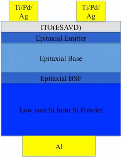
| Fig 1. Schematic of the solar cell structure |
|
Latest results
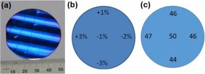
| Fig 2. Photo and sheet resistance results for As-deposited onto ITO deposited on onto Si wafers: As-deposited 80 nm thickness ITO deposited on onto Φ50 mm Si wafers (a) photo, (b) thickness variation silicon wafer; (c) sheet resistance variation (unit: Ω/☐) |
|
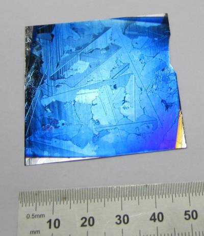
| Fig 3. Photo of solar cell device of thin Si layer based solar cells with diffused emitter ITO layer and Tandem Structure of an all-solid state lithium-ion battery |
 |
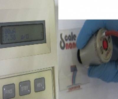
| Fig 4. Transparent conducting thin film based on Ag nanowire based compositer |
|
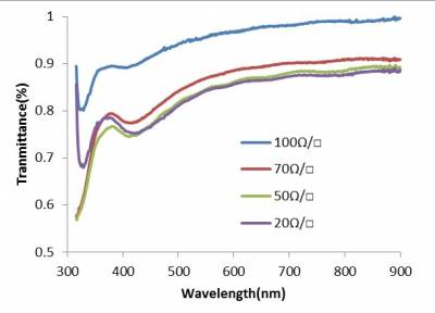
| Fig 5.Transmittance of conducting thin film based on Ag nanowire based composite |
|
Patents
- Mingqing Wang · K.L Choy "Transparent electrodes" Ref. No: GB1309673.0

 Close
Close

