Scanning Electron Microscopy
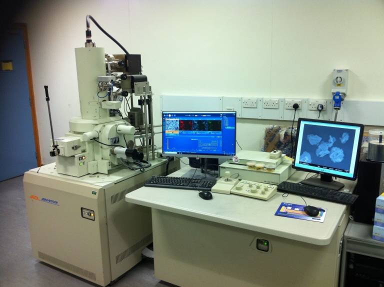
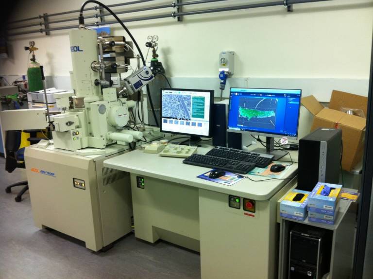
All three have field emission guns (FEGs) and the instrumental resolution is about 2 – 3 nm as measured on gold particles sputtered onto a carbon substrate. However, this resolution is rarely achieved on users’ samples due to sample charging or beam damage effects. All three SEMs are equipped with Oxford Instruments EDS detectors.


It is critically important that samples are non-magnetic. The incoming electrons are focused on the sample surface by magnetic lenses, and the sample sits in a powerful magnetic field. If the sample is magnetic it will be attracted to the lower focusing lens (the objective polepiece) and stick to it. The magnetic field of this sample will then distort the trajectory of the electrons, making focusing impossible. The polepiece will have to be cleaned, which can only be done by an engineer, so it will take a week or more. It is possible that the polepiece cannot be cleaned so will have to be replaced. This will take even more time and will be very expensive. If the sample is a fine powder, it will get accelerated past the polepiece into the column of the microscope, making the cleaning more difficult and time consuming.
For this reason, NO magnetic material can be put into these SEMs. It is easy to check a sample to see if it is magnetic by using the neodymium magnet kept by the sample preparation table at the far end of LG27. Potentially magnetic materials MUST be tested BEFORE sample preparation. That is the test MUST be done on the bulk powder, not after it has been put on a stub. The most common elements forming magnetic compounds are iron, cobalt and nickel. ALL samples containing these elements MUST be tested before sample preparation. Samples containing more unusual but potentially magnetic elements such as neodymium or gadolinium must also be tested. Anybody who puts an untested sample containing any of these elements into the SEM will be BANNED from future use, even if the sample turns out to be non-magnetic.
The SEM sample chambers operate at low pressure (less that 3 x 10 -4 Pa), so the samples have to be dry before sample preparation.
To produce good SEM images, the sample surface has to be electrically conducting. This is because the SEM works by scanning a focused beam of electrons across the sample surface, and those electrons have to be able to move away to the electrical earth (the sample stub) before the next scan. These electrons can easily move if the sample surface is conducting, but not if it is an insulator. For an insulating surface the electrons cannot move and so build up on subsequent scans. These electrons are loosely bound to the sample surface and so are easily ejected and add to the secondary electrons that are used to form the image. This results in very bright areas in the image, often bright enough to saturate the detector. Most materials are not electrically conducting so need to be coated with a conducting material. We have two coaters; a resistance heater for carbon coating, and a sputter coater for gold coating. For SEM imaging, gold coating usually gives better results. Being a relatively heavy element, gold has a high secondary electron yield and so produces good SEM images. However, gold is not so good for EDS analysis. The gold layer will partially block the x-rays used for EDS, blocking the lower energy x-rays more that the higher energy ones, and so will distort the EDS spectrum. This is not be a problem for EDS imaging, where the elemental distribution and not the ratio is of interest. If gold is not appropriate, then carbon coating can be used. The SEM images might not be so good, but the elemental ratios from EDS will be more reliable.
Before going into the SEM, samples are attached to a 25 mm diameter aluminium disk (a stub) and are held in place with a circular piece of double-sided carbon tape (a tab). If the sample is a powder, a small amount is placed onto the tab, the excess is tapped off and then the sample is gold or carbon coated if necessary. If the sample is a thin film on a substrate, the substrate is pressed onto the tab. It must fit inside the area of the stub, there cannot be any of the substrate over the edge of the stub. Thin strips of copper tape are then added to make sure there is good electrical contact between the sample surface and the stub, which is then gold or carbon coated as appropriate. When coated, the stubs are placed into a sample holder to go into the SEM sample chamber. ALWAYS wear gloves when handling the sample holder.
When the session is finished and the sample removed from the chamber, the images are copied from the pc onto a DVD. The pc cannot be connected to the internet, because this would interfere with the communication between the microscope and the pc. With no internet, there is no antivirus software and so USB flash drives must NEVER be used on these pcs. The images are copied onto DVDs, and there are always some available in the lab.
For training, contact s.firth@ucl.ac.uk. The training will take two to three hours and will be done using one of your samples. The rest of the session will be spent practicing on your other samples. Training has to be done individually, one person at a time.
 Close
Close

