Close
Close

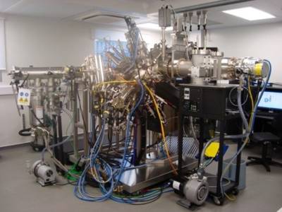
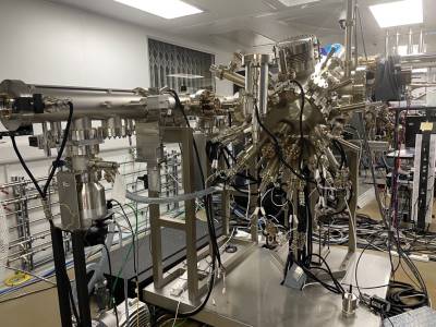
Veeco GEN 930 Twin Chamber System:
Two Veeco GEN 930 chambers working on different materials have been connected with a vacuum chamber in UCL. The advantage of this twin chamber system is the epitaxial growth capability of III-V material and group IV material. Wafers can be grown in the group IV chamber and then transferred into the III-V chamber for further III-V growth under a high vacuum.
See more details of III-V MBE and Group IV MBE here.
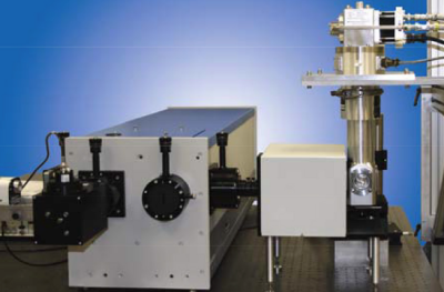
Nanometrics RPM2000 rapid photoluminescence mapper:
The rapid photoluminescence mapper is a Nanometrics RPM2000, and was installed in 2010. This system has been fully functional for daily use in the quality control of epitaxy wafers since its installation. The RPM2000 has been equipped with three lasers (532 nm, 635 nm, and 980 nm) and two detectors (CCD and extended InGaAs detectors) to cover a wide measurement range from around 600 to 2100 nm. The system is also specifically designed to accommodate both small samples and whole wafers (up to 6 inches). The RPM2000 is capable of producing high spatial (100 µm) and spectral resolution PL mappings, giving true image quality of PL quality of epi-wafers.
Temperature-dependent photoluminescence measurement:
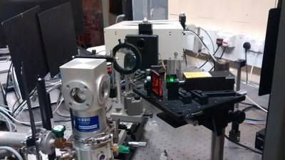
Our self-setup photoluminescence measurement has a 532-nm green laser as the exciting source, Si and Ge detector which has different coverage on wavelength. The vacuum pump and liquid helium compressor provide temperature-dependent measurements from 10K to room temperature.
Jordan Valley D1 X-ray diffraction instrument:
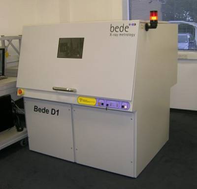
he XRD instrument is a D1 system from Jordan Valley, and was installed in 2010. This system is a flexible and fast operating system for MBE-grown thin-film materials research and quality control. The system is currently fully functional and in excellent condition. The system has fully automated source optics for rapid measurements, and for switching between different modes, e.g. from standard XRD to High-Resolution mode, without user intervention. The system has a robust 5-axis Eulerian cradle capacity for wafer mapping up to 6 inches.
The micro-PL setup will be finished soon.
This system uses MY20X-824 20 x objective lens within the range between 480 nm to 1800 nm. The spectral resolution for this system is down to 0.006 nm for photoluminescence. The system is also interfaced with a semiconductor chiller for temperature-dependent measurement from around 77 K to 300 K.
Felcon laminar flow wet bench: There are two Felcon laminar flow wet benches installed with the MBE systems in 2010 to provide an ultra-clean (class 100) area for sample preparation for MBE growth.
Bentham spectral responsivity system: The Bentham spectral responsivity system is a newly acquired custom-designed equipment for measuring spectral responsivity for wavelengths up to 20 µm. The system is interfaced with a Janis CCS150 closed-cycle cryostat for temperature-dependent measurement from 10 to 350 K.
Bentham Mid-IR PL Measurement System: Bentham Mid-IR PL Measurement System was set up in 2015, and is designed for the PL measurement at mid-IR wavelength. The system is also interfaced with a Janis CCS150 closed-cycle cryostat for temperature-dependent measurement from 10 to 350 K.
Veeco GEN 930 MBE systems
Veeco GEN 930 III-V MBE
UCL III-V MBE system has three group-III sources including Indium, Gallium and Aluminium; three group V sources include Phosphorus, Arsenic and Antimony; doping cells Silicon and Beryllium. The system has been installed in UCL since 2009. High-quality III-V materials grown on Si have been developed on this machine especially III-V quantum dots laser and self-catalysed nanowire on Si. High-performance InP-based, GaAs-based and III-Sb devices also have been carried out by this machine during the past years.
The uniqueness of this MBE system is the compatibility of Phosphorus, Arsenic and Antimony, which could cover the wavelength from visible to Mid-IR. A Phosphorus Recovery System pumps out the residual phosphorus after the growth. Currently, the projects we are working on based on this system include quantum dot semiconductor lasers on InP and Si, Self-catalysed nanowires on Si, solar cells, detector and etc.
This system is capable of growing high-quality III-V materials on native substrates and Group IV substrates such as Si and Ge. In addition, high-performance QD, as well as QD lasers, have been achieved based on this system. In addition, dislocation filter layers have also been investigated.
Figure 1
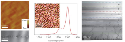
Figure 1: Left: high quality III-V material directly grown on the Ge substrate. Middle: Narrow linewidth of photoluminescence showing high uniformity InAs quantum dots grown on Si substrate Right: five sets of defect filter layers successfully reduced the threading dislocation density for III-V materials grown on Si substrate.
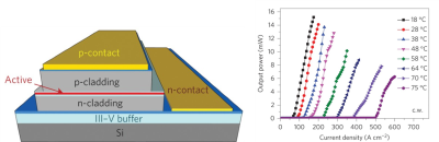
The schematic diagram shows fabrication quantum dot laser grown on Si substrate. The graph shows light against against current curve for Si-based InAs/GaAs quantum dot laser with different temperature conditions
Veeco GEN 930 Group-IV MBE
The Veeco GEN 930 Group IV MBE system was installed in December 2016. The system has two Silicon sources (effusion and e-beam), Germanium, Tin, Boron (doping) and Antimony (doping) cells. The system was shipped to UCL in Oct 2015.
The Veeco Gen930 system has three main vacuum chambers: the loadlock chamber, the prep chamber and the growth chamber. The chambers are separated with ultra-high vacuum (UHV) gate valves to prevent cross-contamination. The system is equipped with an ultra-high vacuum 100cc e-beam evaporator with in-situ deposition monitoring for the deposition of Si. Standard K-cells are used for the evaporation of Ge, Tin and B, while a dual-zone cracking cell is used for Sb. A Reflective High Energy Electron Diffraction (RHEED) system is used to monitor the growth in‑situ. This system is capable of growing Si, Ge, Sn and their alloys, with low-dimensional structure types, including quantum dots, nanowires and quantum wells.
The system is capable of growing high-quality silicon epilayers, as confirmed by the RHEED pattern and AFM measurements. The RMS roughness of 0.077 nm has been calculated. Such high-quality silicon growth is essential for the development of high-performance group-IV-based devices.
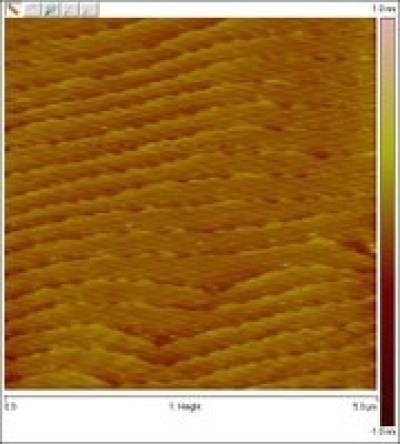
Figure 3: AFM images of very flat (RMS roughness: 0.77 nm) Si epilayers grown on Si substrate
The system has also been used to successfully grow Ge epilayers directly on Si wafers. A 250-nm-thick buffer layer grown using a two-step growth method has an RMS roughness of approximately 0.1 nm.
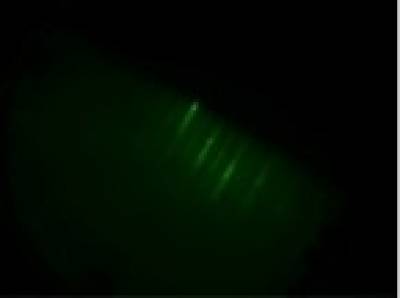
Figure 4: Image of Reflective high energy electron diffraction, showing an atomic reconstruction of Ge epilayers on Si substrate
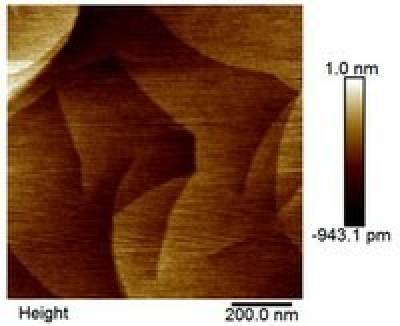
Figure 5 : AFM images of very flat (RMS roughness: 0.77 nm) Si epilayers grown on Si substrate
Quantum structures like Ge/Si superlattices have been grown using this MBE system. An XRD measurement of a superlattice consisting of ten periods of 20 nm of Si and 2 monolayers of Ge show multiple periodic peaks corresponding to reflections off the Ge/Si interfaces in the superlattice. This indicates that the lattice is of high quality, layers thicknesses are consistent and the interfaces are sharp
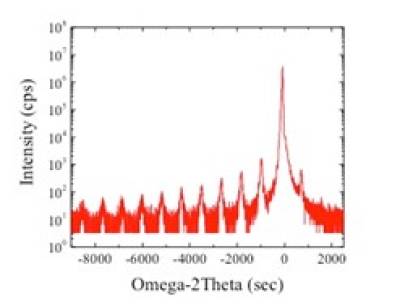
Figure 6 : High resolution x-ray diffraction measurement of high quality GeSi superlattice.
Veeco GEN 930 QD MBE
A brand new GEN 930 III-V MBE system has three group II sources including Indium, Gallium and Aluminium; one group V source --- Arsenic; doping cells Silicon and Beryllium. This machine focuses on growing high-performance InAs/GaAs Quantum Dot lasers on native substrates as well as Si substrates in order to fulfil the high-performance InAs/GaAs QD lasers on Si substrates.
With the help of this brand-new III-V machine with a clean and high-vacuum chamber, we have achieved high-performance InAs/GaAs QDs, which have a density of over 600 /um2 and an FWHM as narrow as 29 meV.
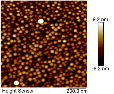
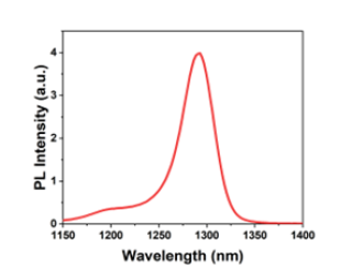
Figure 7 : Optimised high-quality InAs QDs grown on GaAs substrate. Left: The QD morphology in the central 1 um2 area, which has over 550 QDs with high uniformity. Right: The high PL intensity around 1.3 um of the central part
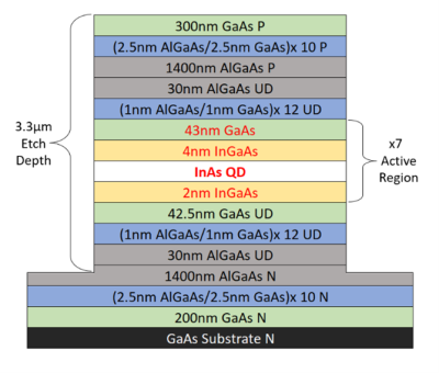
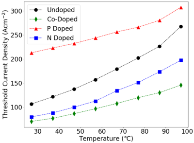
Apart from high-performance QDs, doping strategies for InAs QD lasers have also been researched based on this system. Co-doping technique, which combines direct n-type doping and modulation p-type doping, has been proposed to achieve a much lower threshold current density compared to the solely doped and undoped QD lasers.