 Close
Close

Building quantum processors using industrial mass fabrication techniques
31 March 2021
UCL-led research reports the first measurements of a single electron spin in a device fabricated using 300mm wafer scale processing.
Quantum computers promise to solve some of the most challenging computational problems, such as revolutionising communications and the search for new materials, chemicals and medicines.
However, to tackle the most demanding computational simulations, it is thought that a large-scale fault-tolerant quantum computer might ultimately require 10 million quantum bits (qubits) - a much larger number than current technology can support. The monumental task consists of not only fabricating so many qubits, but also controlling them independently and selectively tuning their inter-qubit interaction.
One of the first requirements to unleash the full potential of quantum computing is the reproducibility and homogeneity of the devices where qubits are contained. The answer to this challenge could be silicon transistors, like the ones found in any mobile smart phone or laptop.
Silicon transistor fabrication techniques have been developed and improved over decades and can now routinely manufacture billions of transistors per chip. These developments in industrial silicon fabrication techniques (known as CMOS) motivates the quantum hardware research in silicon quantum dots formed in devices fabricated using CMOS techniques. It is hoped that this form of quantum hardware will reach the required number and density of qubits.
Today, UCL researchers along with researchers from UCLQ spin-out Quantum Motion, CEA LETI, Hitachi Cambridge Laboratory, and Université Grenoble Alpes report in PRX Quantum the first measurement of an electron spin in a singly-occupied gate-defined quantum dot, fabricated using CMOS compatible processes at the 300 mm wafer scale. The long relaxation times over several seconds measured, show a great deal of promise for these devices.
The UCLQ team and their colleagues found that on a single split-gate transistor, they could demonstrate sensitive and compact spin readout. They measured the spin polarisation of a single electron confined in the dot formed under one of the gates using spin dependent tunnelling to convert the spin degree of freedom into a charge tunnelling event. The dot formed under the other gate was used as a charge sensor.
Corresponding author, Virginia Ciriano-Tejel, and student of the EPSRC Centre for Doctoral Training in Delivering Quantum Technologies said: “Our work addresses two issues, first evaluating whether CMOS-compatible manufacturing processes performed at the scale of 300mm wafers can be used to make long-lived spin qubits, and secondly, whether this is possible when combined with a reduced-footprint readout method.”
The long relaxation times and compactness of the spin-readout circuit confirm that silicon transistors, once at the heart of the digital revolution can have a second golden era as the vessel for spin electron qubits.
Director of UCLQ and co-founder of Quantum Motion, Professor John Morton says: “Silicon electronics has already transformed our society over the past decades, and it has huge potential to deliver the scalable platform that can realise the most profound impacts of quantum computing.”
This research received funding from the UK Engineering and Physical Sciences Research Council and the European Union’s Horizon 2020 research and innovation programme, with additional support from the Royal Society and Telefónica British-Spanish Society.
Links:
- Read the paper at PRX Quantum
- Read the UCL Press Release
- Read news article from Sifted
- Visit the website of UCL’s Quantum Spin Dynamics group
- Find out more about the EPSRC Centre for Doctoral Training in Delivering Quantum Technologies
- Find out more about quantum research at UCL
- Find out more about Quantum Motion
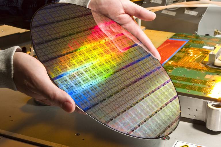
Image caption:
Photo of a CMOS fabricated 300mm wafer (Credit: CEA LETI).