Suit up!
22 July 2013

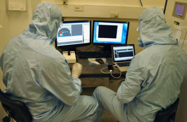
Inside the cleanroom at the London Centre for Nanotechnology, protective gear is required everywhere. Jumpsuits, special boots and protective glasses don't just have to be worn when manipulating equipment or samples. Scientists using the cleanroom must cover up even when using computer equipment, to prevent any dust from entering the facility.
In this photo, two researchers are using the computer console that operates the Raith 150-TWO Electron Beam Lithography system. Next to the console, to the right of the operators, is a metal enclosure the size of a large wardrobe, which contains the high-tech equipment. Electron beam lithography systems are used to mark nano-scale designs onto the surface of semiconductor wafers - useful for making computer chips and other related technologies.
The machine works by shining a beam of electrons onto the wafer, marking out the design on the its coating. Later, the wafer is bathed in acid, etching the design into the surface.
Unlike photolithography, a similar technique where light marks out the designs on a chip's surface, electron beam lithography can produce finer, more detailed designs. This is because, on very small scales, light cannot be focused perfectly: there is always some degree of fuzziness, or diffraction, where the light beam spreads out. Electron beams suffer far less from this phenomenon, but producing chips using this method is much slower, particularly on industrial scales.
Photo credit: O. Usher (UCL MAPS)
Links
High resolution image
This image can be reproduced freely providing the source is credited
 Close
Close


