 Close
Close

Perfectly-absorbing photoconductive metasurface significantly improves THz detectors
3 May 2019
UCL Electronic and Electrical Engineering research featured in Nano Letters and Nanowerk highlights new photoconductive metasurface integrated into THz detectors.
UCL Electronic and Electrical Engineering research featured in Nano Letters and Nanowerk highlights new photoconductive metasurface integrated into THz detectors. Work involves two Centre for Doctoral Training (CDT) PhD students from the UCL-Imperial Materials Characterisation CDT and the UCL-Cambridge Integrated Photonic and Electronic Systems CDT. UCL EEE is leading on one CDT and partner on three others.
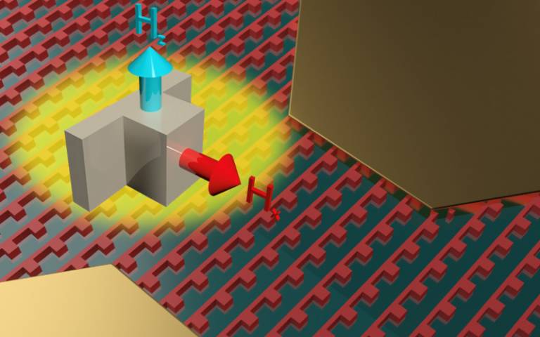
Dr Oleg Mitrofanov, Reader in Terahertz (THz) Photonics at UCL EEE and his PhD students Tom Siday (Materials Characterisation CDT) and Lucy Hale (IPES CDT) have developed an all-dielectric perfectly-absorbing photoconductive metasurface, which has significantly improved the efficiency of THz photoconductive detectors. The metasurface consists of a network of photoconductive nanostructures, which efficiently absorb light at a designed wavelength, and as a result the metasurface conductivity can be changed from a highly resistive to a highly conductive state on the sub-picosecond time scale.
The metasurface enables a combination of optical and electronic properties, which is optimal for photoconductive THz detectors, and which is difficult to realise with conventional materials. The researchers believe that the metasurface concept can be applied also for a range of applications, for example efficient fast modulators and THz emitters.
While perfectly-absorbing metasurfaces have been developed in the past, most commonly using a metallic reflector within the structure, it is often impossible to use this design in practical THz devices due to electrical conductivity of the metallic layer. Only recently, an alternative idea, which does not require a reflector was proposed: it is based on an interplay of two Mie modes, the fundamental electromagnetic field resonances geometry the structure defined. In their recent work, published in Nano Letters, the researchers show for the first time that perfect absorption can be realised using two Mie magnetic dipole modes, oriented orthogonally to each other and displaying different symmetry (odd and even).
You can also read the articles