Close
Close

HOME | Vacancies | MEMBERS | Publications | LINKS |
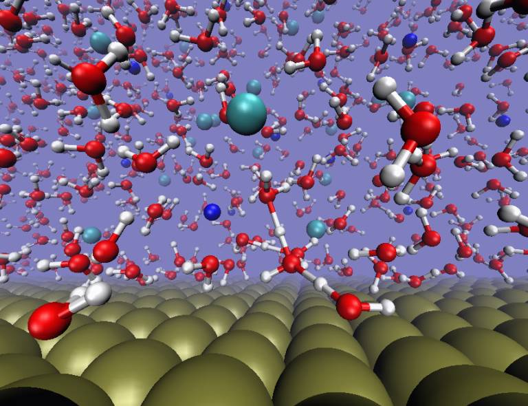
Photo-induced desorption of atoms and ions from surfaces of ionic materials
Electronic excitations of solids create bulk and surface defects can induce surface decomposition and particle emission and lead to desorption of adsorbed species. Techniques such as desorption induced by electronic transitions (DIET), laser ablation and photon-induced desorption have many technological applications. Irradiation sources used in these techniques include ion and electron beams, x-rays and lasers. These induce a variety of defect formation processes that are difficult to distinguish or control. One of the major challenges, therefore, is to understand the mechanisms of defect formation, diffusion and interconversion under the given irradiation conditions and to achieve control over the desorption products.
Electronic processes in novel electro-active materials
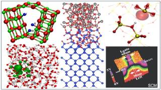
Most of the transparent materials are insulators and most of the conductive materials are non-transparent. Combination of the optical transparency and electrical conductivity is a very useful and rare property. It has been recently discovered that a complex oxide 12CaO ;middot 7Al2O3 (known as C12A7) can be converted from an insulator to a conductor in several different ways. The unusual structure of C12A7 defines many of its properties including electride state, i.e. a material in which electrons serve the role of anions. Applications of C12A7 include O- "gun" (emitter of highly reactive O- species) and cold electron emitter based on C12A7 electride (workfunction of C12A7 electride is only 0.6 eV). In addition, C12A7 doped with H can be reversibly converted from an insulator to an electrical conductor using light forming a new class of transparent conducting oxides.
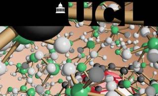
Structure and properties of defects in materials
Understanding of the structure and electronic properties of defects at oxide surfaces is crucial for their applications as substrates, sensors, catalysts, and coatings. The role of the low-coordinated surface sites such as steps and kinks as well as surface vacancies and divacancies is well appreciated. However, a clear correlation between the structure of surface features and their electronic properties is still lacking. I address basic questions relevant to the charge and energy transfer processes: what are the optical absorption energies, ionisation potentials and electron affinities of typical surface features and how the electrons and holes are localised at the low-coordinated sites. I also consider photo-induced formation of transient chemically active species and mechanisms of chemical reactions.
Adsorption and diffusion of molecules at surfaces
The adsorption and diffusion of organic molecules on surfaces are integral to many areas of surface science and nanotechnology, such as self-assembly and growth of new surface structures, catalysis, coatings, corrosion inhibition, tribology, and molecular electronics. The advent of scanning probes sparked an explosion of interest in studying the behavior and reactions of individual molecules at surfaces.
Embedded cluster approach for studies of defects and defect processes in insulators
Calculations of defects and defect processes in materials have to account accurately for several physical phenomena such as (depending on the problem) trapping of electronic charge, mechanisms of defect formation, defect induced relaxation, photo-induced excitations and formation of transient species. There are three models that are usually used in calculations. In the periodic model a fragment of a material (supercell) is selected and translated periodically in three dimensions. In a molecular cluster model a finite fragment of material (cluster) is used to model the defect and its nearest environment. Both schemes have their pros and cons. The embedded cluster model attempts to combine the advantages of both of them. In this case a defect with its nearest environment is considered using a high-level theory (usually ab initio methods). At the same time the effect of the remaining part of the system is taken into account using a less accurate method, e.g. classical inter-atomic potential. One of such schemes has been pioneered at UCL and is now implemented is a computer code GUESS (Gaussians used for Embedded System Studies). Further development of the embedded cluster approach is in the focus of our research program.
Defects in polycrystalline metals
The formation of voids due to the thermal stress loading of metal films has a detrimental effect on the performance of electronic devices, eventually leading to complete failure. Voids, the most commonly occurred defects under such conditions, are thought to be formed by the aggregation of vacancies. However, the mechanism via which vacancies aggregate to form voids is not fully understood. We combine the efficiency of Molecular Dynamics and semi-empirical/empirical forcefields with the accuracy of density functional theory (DFT) methods to address the issue of degradation effects in Cu at a multi-scale level.