Close
Close

Our research is focused on the development and application of theoretical methodologies for calculations of defects and defect related processes in solids and at interfaces.

Members | Research | Publications | Vacancies | Links |
- We develop atomistic theories of the geometric and electronic structure of point defects and the mechanisms of electronic and ionic processes in insulators and semiconductors, in particular for microelectronics applications.
- We create models of trapped excitons and electron and hole polarons in solids and at surfaces and develop mechanisms of photo-induced processes at ionic surfaces and in metal nanofilms.
- We develop theoretical methods for modelling of Atomic Force Microscopy imaging of surfaces and the mechanisms of contrast formation in AFM images in vacuum and in liquids.
- We model adsorption and diffusion of organic molecules at insulating surfaces and mechanisms of formation of molecular super-structures and self-assembled monolayers.
Recent Highlights
Modeling the Effects of Varying the Ti Concentration on the Mechanical Properties of Cu–Ti Alloys
Fotopoulos, V., O'Hern, C.S., Shattuck, M., Shluger, A.L.
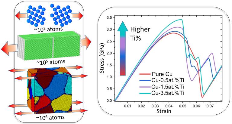
The mechanical properties of CuTi alloys have been characterized extensively through experimental studies. However, a detailed understanding of why the strength of Cu increases after a small fraction of Ti atoms are added to the alloy is still missing. In this work, we address this question using density functional theory (DFT) and molecular dynamics (MD) simulations with the modified embedded atom method (MEAM) interatomic potentials. First, we performed calculations of the uniaxial tension deformations of small bicrystalline Cu cells using DFT static simulations. We then carried out uniaxial tension deformations on much larger bicrystalline and polycrystalline Cu cells by using MEAM MD simulations. In bicrystalline Cu, the inclusion of Ti increases the grain boundary separation energy and the maximum tensile stress. The DFT calculations demonstrate that the increase in the tensile stress can be attributed to an increase in the local charge density arising from Ti. MEAM simulations in larger bicrystalline systems have shown that increasing the Ti concentration decreases the density of the stacking faults. This observation is enhanced in polycrystalline Cu, where the addition of Ti atoms, even at concentrations as low as 1.5 atomic (at.) %, increases the yield strength and elastic modulus of the material compared to pure Cu. Under uniaxial tensile loading, the addition of small amounts of Ti hinders the formation of partial Shockley dislocations in the grain boundaries of Cu, leading to a reduced level of local deformation. These results shed light on the role of Ti in determining the mechanical properties of polycrystalline Cu and enable the engineering of grain boundaries and the inclusion of Ti to improve degradation resistance.
On the Structure of Oxygen Deficient Amorphous Oxide Films
Strand, J., Shluger, A.L.
Advanced Science, December 2023
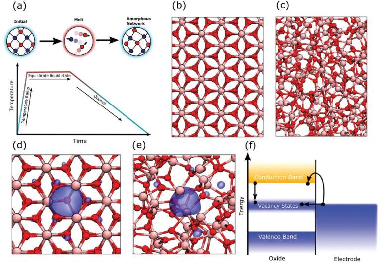
a) Schematic of the melt-and-quench process use to generate pseudo-amorphous models. b) The alpha-phase of Al2O3(corundum). c) A samplemodel of a-Al2O3. d) A model of an oxygen vacancy in alpha-Al2O3. e) A model of an oxygen vacancy in a-Al2O3. The blue surface is an iso-surface of the in-gap one-electron state of the vacancy. f) Schematic of the band allignment of an oxide containing oxygen vacancies with a metal electrode.Defects, such as vacancies, produce in-gap states. Electrons from the conduction band or from a nearby electron source (e.g., electrode) can transferinto the vacancy states via capture (from the conduction band) or tunnelling (from an electrode). Peach ions indicate Al, red ions indicate O.
Understanding defects in amorphous oxide films and heterostructures is vital to improving performance of microelectronic devices, thin-film transistors, and electrocatalysis. However, to what extent the structure and properties of point defects in amorphous solids are similar to those in the crystalline phase are still debated. The validity of this analogy and the experimental and theoretical evidence of the effects of oxygen deficiency in amorphous oxide films are critically discussed. The authors start with the meaning and significance of defect models, such as “oxygen vacancy” in crystalline oxides, and then introduce experimental and computational methods used to study intrinsic defects in amorphous oxides and discuss their limitations and challenges. To test the validity of existing defect models, ab initio molecular dynamics is used with a non-local density functional to model the structure and electronic properties of oxygen-deficient amorphous alumina. Unlike some previous studies, the formation of deep defect states in the bandgap caused by the oxygen deficiency is found. Apart from atomistic structures analogous to crystal vacancies, the formation of more stable defect states characterized by the bond formation between under-coordinated Al ions is shown. The limitations of such defect models and how they may be overcome in simulations are discussed.
Structure and Migration Mechanisms of Small Vacancy Clusters in Cu: A Combined EAM and DFT Study
Fotopoulos, V., Mora-Fonz, D., Kleinbichler, M., Bodlos, R., Kozeschnik, E., Romaner, L., Shluger, A.L.
Voids in face-centered cubic (fcc) metals are commonly assumed to form via the aggregation of vacancies; however, the mechanisms of vacancy clustering and diffusion are not fully understood. In this study, we use computational modeling to provide a detailed insight into the structures and formation energies of primary vacancy clusters, mechanisms and barriers for their migration in bulk copper, and how these properties are affected at simple grain boundaries. The calculations were carried out using embedded atom method (EAM) potentials and density functional theory (DFT) and employed the site-occupation disorder code (SOD), the activation relaxation technique nouveau (ARTn) and the knowledge led master code (KLMC). We investigate stable structures and migration paths and barriers for clusters of up to six vacancies. The migration of vacancy clusters occurs via hops of individual constituent vacancies with di-vacancies having a significantly smaller migration barrier than mono-vacancies and other clusters. This barrier is further reduced when di-vacancies interact with grain boundaries. This interaction leads to the formation of self-interstitial atoms and introduces significant changes into the boundary structure. Tetra-, penta-, and hexa-vacancy clusters exhibit increasingly complex migration paths and higher barriers than smaller clusters. Finally, a direct comparison with the DFT results shows that EAM can accurately describe the vacancy-induced relaxation effects in the Cu bulk and in grain boundaries. Significant discrepancies between the two methods were found in structures with a higher number of low-coordinated atoms, such as penta-vacancies and di-vacancy absortion by grain boundary. These results will be useful for modeling the mechanisms of diffusion of complex defect structures and provide further insights into the structural evolution of metal films under thermal and mechanical stress.
Defects in WS2 monolayer calculated with a nonlocal functional: any difference from GGA?
Kieczka D., Durrant, T., Milton, K., Goh, K.E., Bosman, M., Shluger, A.L.
Electronic Structure, April 2023
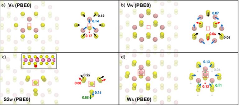
Lattice distortions induced by 4 intrinsic defects in monolayer WS2. Arrows in the figure show the directions of atomic displacements, the values of which are given in Å. Values have been calculated with PBE0 and colour coordinated to the displacement arrows. The defective site is indicated by the red dotted box. Showing the (a) Vs defect (the dotted arrow is the displacements out of plane) (b) Vw defect (c) S2w defect (the inset is the side view of the defect with red defective sulphur atoms) (d) Ws defect.
Density functional theory (DFT) with generalised gradient approximation (GGA) functionals is commonly used to predict defect properties in 2D transition metal dichalcogenides (TMDs). Since GGA functionals often underestimate band gaps of semiconductors and incorrectly describe the character of electron localisation in defects and their level positions within the band gap, it is important to assess the accuracy of these predictions. To this end, we used the non-local density functional Perdew—Burke—Ernzerhof (PBE)0-TC-LRC to calculate the properties of a wide range of intrinsic defects in monolayer WS2. The properties, such as geometry, in-gap states, charge transition levels, electronic structure and the electron/hole localisation of the lowest formation energy defects are discussed in detail. They are broadly similar to those predicted by the GGA PBE functional, but exhibit numerous quantitative differences caused by the degree of electron and hole localisation in charged states. For some anti-site defects, more significant differences are seen, with both changes in defect geometries (differences of up to 0.5 Å) as well as defect level positions within the band gap of WS2. This work provides an insight into the performance of functionals chosen for future DFT calculations of TMDs with respect to the desired defect properties.
Thermodynamic analysis of the interaction between metal vacancies and hydrogen in bulk Cu
Fotopoulos, V., Grau-Crespo, R. and Shluger, A.L.
Physical Chemistry Chemical Physics, March 2023
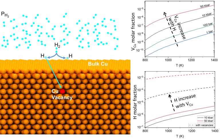
Using grand canonical thermodynamic analysis with inputs from DFT calculations we calculated equilibrium molar fractions of copper vacancies (VCu), H interstitials (Hi) and their complexes in bulk Cu in a wide range of temperature and hydrogen pressure values. The results show that the equilibrium molar fractions of both VCu and Hi are low in most conditions of interest, in good agreement with available experimental data. Although Hi–VCu complexes have significantly lower formation energies than the isolated defects, the low molar fraction of H is predicted to have little impact on the rise in vacancy molar fraction for external hydrogen pressures below 100 bar. Only at relatively high hydrogen pressures exceeding 10 kbar in the presence of Cu vacancies, the H molar fraction was found to reach the same order of magnitude as the molar fraction of vacancies. These results put thermodynamic limits on the hydrogen-induced vacancy clustering and void formation in bulk Cu.
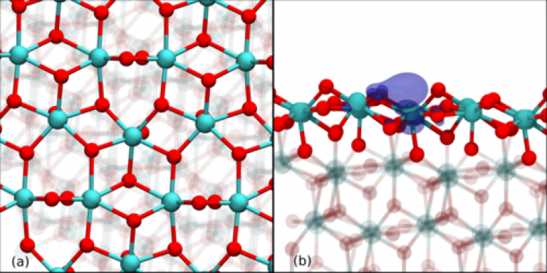
Difference in Structure and Electronic Properties of Oxygen Vacancies in alpha-Quartz and alpha-Cristobalite Phases of SiO2
Milton, K., Durrant, T.R., Cobos Freire, T. and Shluger, A.L.
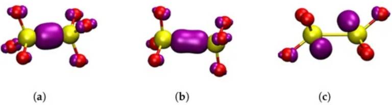
Square modulus of the wavefunction of the highest occupied state in the studied dimer oxygen defects in alpha-C shown in purple. Yellow atoms are silicon and red atoms are oxygen. (a) neutral dimer configuration. (b) positive dimer. (c) negative dimer. (a–c) are general HOMOs applicable to either alpha-cristobalite or alpha-quartz.
alpha-cristobalite (alpha-C) is a polymorph of silica, mainly found in space exploration and geochemistry research. Due to similar densities, alpha-C is often used as a proxy for amorphous SiO2, particularly in computer simulations of SiO2 surfaces and interfaces. However, little is known about the properties of alpha-C and its basic oxygen defects. Using density functional theory (DFT) simulations we provide a comprehensive report on the properties of perfect structure and oxygen vacancies in alpha-C. The calculated properties of alpha-C are compared with those of the better-characterized alpha-quartz (alpha-Q). Our results demonstrated that the positively charged O vacancy in alpha-C is most stable in the dimer configuration, in contrast to alpha-Q, which favors the puckered configuration. A back-projected configuration was also predicted in both polymorphs. We calculated the optical transition energies and isotropic hyperfine constants for O vacancies in both alpha-Q and alpha-C, and compared our findings with the results of previous studies and experiments. This work, thus, offers one of the first in-depth investigations of the properties of oxygen vacancies in alpha-C.
Dielectric breakdown in HfO2 dielectrics: Using multiscale modeling to identify the critical physical processes involved in oxide degradation
Strand, J., La Torraca, P., Padovani, A., Larcher, L. and Shluger, A.L.
Journal of Applied Physics, May 2022
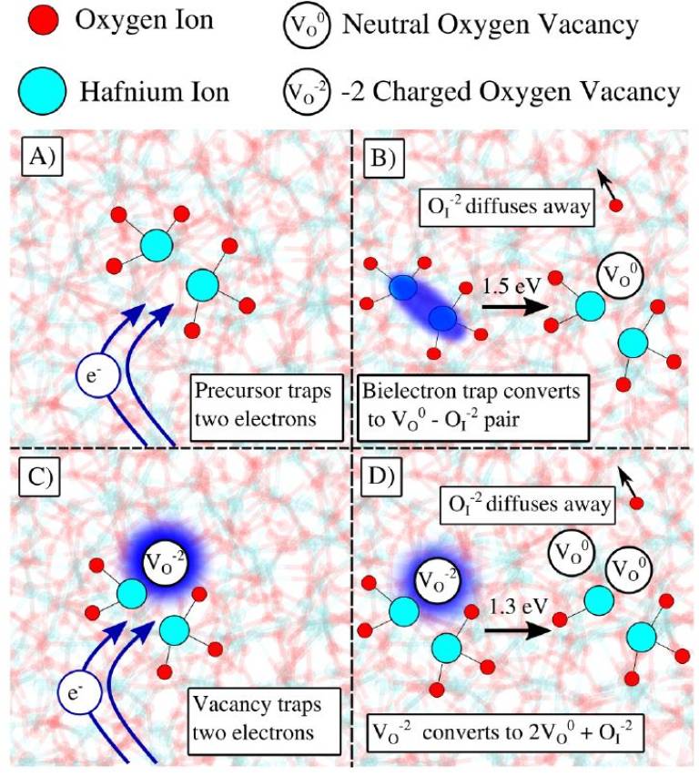
We use a multi-scale modeling to study the time-dependent dielectric breakdown of an amorphous (a-) HfO2 insulator in a metal–oxide–metal capacitor. We focus on the role played by electron injection in the creation of oxygen vacancies, which eventually form the percolation path responsible for dielectric breakdown. In this scenario, the electron transport through the dielectric occurs by multi-phonon trap assisted tunnelling (MPTAT) between O vacancies. Energy parameters characterizing the creation of oxygen vacancies and the MPTAT process are calculated using density functional theory employing a hybrid density functional. The results demonstrate that the formation of neutral O vacancies facilitated by electron injection into the oxide represents a crucial step in the degradation process dominating the kinetics at common breakdown fields. We further show the importance of the so-called “energetic correlation” effect, where pre-existing O vacancies locally increase the generation rate of additional vacancies accelerating the oxide degradation process. This model gives realistic breakdown times and Weibull slopes and provides a detailed insight into the mechanism of dielectric breakdown and atomistic and electronic structures of percolation paths in a-HfO2. It offers a new understanding of degradation mechanisms in oxides used in the current MOSFET technology and can be useful for developing future resistive switching and neuromorphic nanodevices.
Atomistic Modeling of the Electrical Conductivity of Single-Walled Carbon Nanotube Junctions
Durrant, T.R., El-Sayed, A.M., Gao, D., Rueckes, T., Gennadi Bersuker, G., Shluger, A.L.
pss–Rapid Research Letters, June 2022
Energies and structures of Cu/Nb and Cu/W interfaces from density functional theory and semi-empirical calculations
Bodlos, R, Fotopoulos, V, Spitaler, J, Shluger, A.L, Romaner, L.
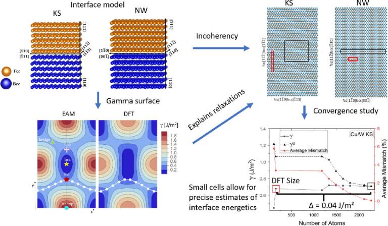
Cu/Me multilayer systems, with Me referring to a body-centered cubic (bcc) metal, such as Nb and W, are widely used for nuclear, electrical, and electronic applications. Despite making up only a small percentage of the volume, interfaces in such systems play a major role in determining their electrical, mechanical, thermal and diffusive properties. Face-centered cubic (fcc) Cu often forms Kurdjumov-Sachs (KS) and Nishiyama-Wassermann (NW) type interfaces with bcc metals or variations thereof. For the Cu/Nb system, these interface relationships have been extensively studied with semi-empirical methods. Surprisingly, the energetics and interface properties of Cu/W have not yet been studied in detail, in spite of extensive applications. In this study, we employ both periodic Embedded Atom Method (EAM) and Density Functional Theory (DFT) simulations to explore the geometric and energetic properties of the KS and NW interfaces of Cu/Nb and Cu/W. To assess the reliability of our approach, the dependence of the results on the size of periodic cells is examined for coherent and incoherent interfaces. We provide the interface energies and the work of separation for the Cu/W and Cu/Nb interfaces at DFT accuracy. The results of calculations with two EAM potentials are in qualitative agreement with those obtained using DFT and allow investigating the convergence of interfacial properties. These key energetic quantities can be used for future thermodynamic and mechanical modeling of Cu/Me interfaces.
The nature of column boundaries in micro-structured silicon oxide nanolayers
Patel, K., Cottom, J., Mehonic, A., Ng, W.H., Kenyon, A.J., Bosman, M. and Shluger, A.L.
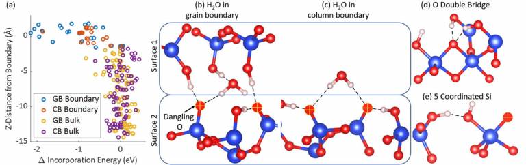
Columnar microstructures are critical for obtaining good resistance switching properties in SiOx resistive random access memory (ReRAM) devices. In this work, the formation and structure of columnar boundaries are studied in sputtered SiOx layers. Using TEM measurements, we analyze SiOx layers in Me–SiOx–Mo heterostructures, where Me = Ti or Au/Ti. We show that the SiOx layers are templated by the Mo surface roughness, leading to the formation of columnar boundaries protruding from troughs at the SiOx/Mo interface. Electron energy-loss spectroscopy measurements show that these boundaries are best characterized as voids, which in turn facilitate Ti, Mo, and Au incorporation from the electrodes into SiOx. Density functional theory calculations of a simple model of the SiO2 grain boundary and column boundary show that O interstitials preferentially reside at the boundaries rather than in the SiO2 bulk. The results elucidate the nature of the SiOx microstructure and the complex interactions between the metal electrodes and the switching oxide, each of which is critically important for further materials engineering and the optimization of ReRAM devices.
Electron trapping in ferroelectric HfO2
Roman A Izmailov, Jack W Strand, Luca Larcher, Barry J O'Sullivan, Alexander L Shluger, Valeri V Afanas' ev
Physical Review Materials, March 2021
Charge trapping study at 300 and 77 K in ferroelectric (annealed Al- or Si-doped) and nonferroelectric (unannealed and/or undoped) HfO2 films grown by atomic layer deposition reveals the presence of “deep” and “shallow” electron traps with volume concentrations in the 1019−cm−3 range. The concentration of deep traps responsible for electron trapping at 300 K is virtually insensitive to the oxide doping by Al or Si but slightly decreases in films crystallized by high-temperature annealing in oxygen-free ambient. This behavior indicates that the trapping sites are intrinsic and probably related to disorder in HfO2 rather than to the oxygen deficiency of the film. Electron injection at 77 K allowed us to fill shallow electron traps energetically distributed at ∼0.2 eV. These electrons are mobile and populate states with thermal ionization energies in the range ∼0.6–0.7 eV below the HfO2 conduction band (CB). The trap energy depth and marginal sensitivity of their concentration to crystallization annealing or film doping with Si or Al suggests that these traps are associated with boundaries between crystalline grains and interfaces between crystalline and amorphous regions in HfO2 films. This hypothesis is supported by density functional theory calculations of electron trapping at surfaces of monoclinic, tetragonal, and orthorhombic phases of HfO2. The calculated trap states are consistent with the observed thermal ionization (0.7–1.0 eV below the HfO2 CB) and photoionization energies (in the range of 2.0–3.5 eV below the HfO2 CB) and support their intrinsic polaronic nature.
Effect of electric field on defect generation and migration in HfO2
Jack W Strand, Jonathon Cottom, Luca Larcher, Alexander L Shluger
Understanding the effect of electric fields on defect creation and diffusion in metal oxides is of fundamental importance for developing accurate models of oxide degradation in electronic devices and dielectric breakdown. We use the Berry phase operator method within density functional theory to calculate how an applied electric field affects barriers for the creation of oxygen vacancy-interstitial defect pairs (DPs) and diffusion of interstitial O ions in monoclinic (m-)HfO2. The results demonstrate that even close to breakdown fields, barriers for DP generation exceed 6 eV in the perfect m−HfO2 lattice. Simulated injection of extra electrons from electrodes significantly lowers barriers for the creation of DPs, which are further reduced by the field to around 1 eV. Thus, bias application facilitates the injection of electrons into the oxide; these extra electrons reduce energy barriers for the creation of O vacancies, and these barriers as well as those for O ion diffusion are further lowered by the field. We find that, within a linear regime, the electric field modulates the barrier height by a dot product between the electric field and the electric dipole at the zero-field transition state to good accuracy.
With the current trend in technology to lower fabrication processing temperatures, extreme bonding geometries in the oxide are expected to become more abundant and increase the influence of strain, ranging from ultra-thin oxides sandwiched between electrodes to porous low-k insulators intrinsically strained by re-bonding reactions. Hence this discovery of unexpected reactivity of atomic hydrogen may have significant implications for the future of silica based device processing.
Contact us
Prof. Alexander Shluger: a.shluger@ucl.ac.uk
Department of Physics and Astronomy, University College London, Gower Street, London WC1E 6BT
Find directions to our department: www.ucl.ac.uk/physics-astronomy/about/find-us